Intel revealed details of its upcoming Tiger Lake mobile processor, along with its associated Willow Cove core, at its Intel Architecture Day event on Aug. 11.
Tiger Lake: new core, new graphics, new features
Tiger Lake is Intel’s next-generation mobile platform and the successor to Ice Lake. Although it’s still built on the 10nm node, Intel claims that Tiger Lake–and its Willow Cove core architecture–will bring performance uplift similar to a node shrink.
During the presentation, Intel noted that it focused on three areas for the Willow Cove core: reworking the caching architecture, improving performance over Sunny Cove core, and keeping it all secure.
And the graphs appeared promising. Intel showed that Willow Cove is expected to reach much higher frequencies at the same voltage levels than Sunny Cove. It projects a much wider dynamic frequency range, seemingly capable of hitting 5GHz at higher voltage levels.
The frequency increase is important. As AnandTech reported, although Sunny Cove is around 18 per cent faster clock-per-clock against the older Skylake core, its ran at lower frequencies that dampened the performance improvements. If Willow Cove can indeed hit the advertised clocks, then the full potential of the architecture can be realized.
The improved power efficiency leaves Tiger Lake with more power and thermal headroom, and what better way to fill that gap than with Intel’s brand new Xe graphics. Intel said that Willow Cove carries up to 96 execution units (EUs) while keeping within the same power envelope as Ice Lake.
Intel processors have been criticized for their lack of next-gen features, and Tiger Lake is looking to change that perception. On the memory front, Intel has increased Tiger Lake’s mid-level cache size from 512 KB to 1.25MB. The last-level cache (LLC) has been expanded by 50 per cent, reducing the need to refer to the slower system memory.
Unsurprisingly, Tiger Lake features a new memory controller that not only supports LP4x/DDR4 memory, but also LPDDR5 memory up to 5,400MHz. Other new features include support for Thunderbolt 4, USB4, PCIe 4, and integrated display output via USB Type-C. Intel emphasized that that PCIe 4 support is on the CPU rather than on the platform controller hub (PCH) to ensure the maximum bandwidth and minimize latency.
For applications that take advantage of AI smarts like Adobe Sensei, Tiger Lake now features an upgraded Gaussian and Neural Accelerator (GNA 2.0). According to Intel, the new accelerator reduces CPU utilization by up to 20 per cent compared to the previous gen.
Related:
Intel launches Lakefield 10nm hybrid processor with Foveros 3D packaging
The transistor transition
Much of Tiger Lake’s improvements stem from a revamped 10nm manufacturing process. It was a such a huge focus that Intel even gave it a fancy new name: SuperFin.
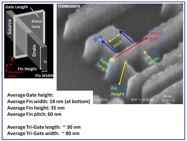
Before digging into SuperFin, here’s a refresher on how a processor transistor works. The transistors in processors are just incredibly small switches that toggle really fast. Processors today almost ubiquitously use field-effect transistors (FET). A FET consists of a source on one end and a drain on the other. Sandwiched between them is a gate, which creates an electron channel between the source and the drain when a voltage is applied to it. Intel’s modified transistors are called FinFET to describe their raised 3D design (shaped like a fin) that replaces the old planar design. The raised fins provide more surface area and prevent electrons from moving across the gate when the gate is closed.

For Tiger Lake, Intel has revised its 10nm FinFET design. First, it reduced the resistance of the source and drain, allowing more current to flow through the channel. Intel has also increased the gate pitch, or space between the gates, to increase the drive current. Lastly, an improved gate process increases channel mobility – how quickly electrons can move across the channel.
In an email to IT World Canada, Intel explained that while the gate pitch impacts the size of the standard cell, it’s only a small part of the various factors that affect density. Design choices, metal routing layers, and many other factors all determine transistor density. Additionally, Intel said that “On the whole, our 10nm SuperFin technology is equivalent in density to foundry 7nm processes.”
Transistors are only part of the equation; the metal stack’s performance is just as important. A metal stack interconnect layer sits on top of the transistors and holds the microscopic circuits that connect all the transistors.
Due to the complex relationships between the transistors, it’s impossible to route all of the wires into a single horizontal plane. To solve this challenge, engineers stacked them into multiple layers, insulating the layer with a barrier. Generally, more complex designs need more wiring and therefore more layers.
Semiconductor engineers are always exploring new methods to increase the metal stack’s electrical efficiency, such as shrinking the wire size, using new materials, and physical redesigns. With that said, even small changes could have an impact on the rest of the design, so changes needed to be made carefully.
When it released its 10nm transistors, Intel replaced copper with cobalt in the metal stack’s first two local layers. The local layers hold the thinnest wires that sit closest to the transistors. Comparatively, cobalt is more electrically resistant than copper, but its barrier requirement is significantly lower. Along with other factors, Intel said that using cobalt reduced voltage via resistance by up to two times.
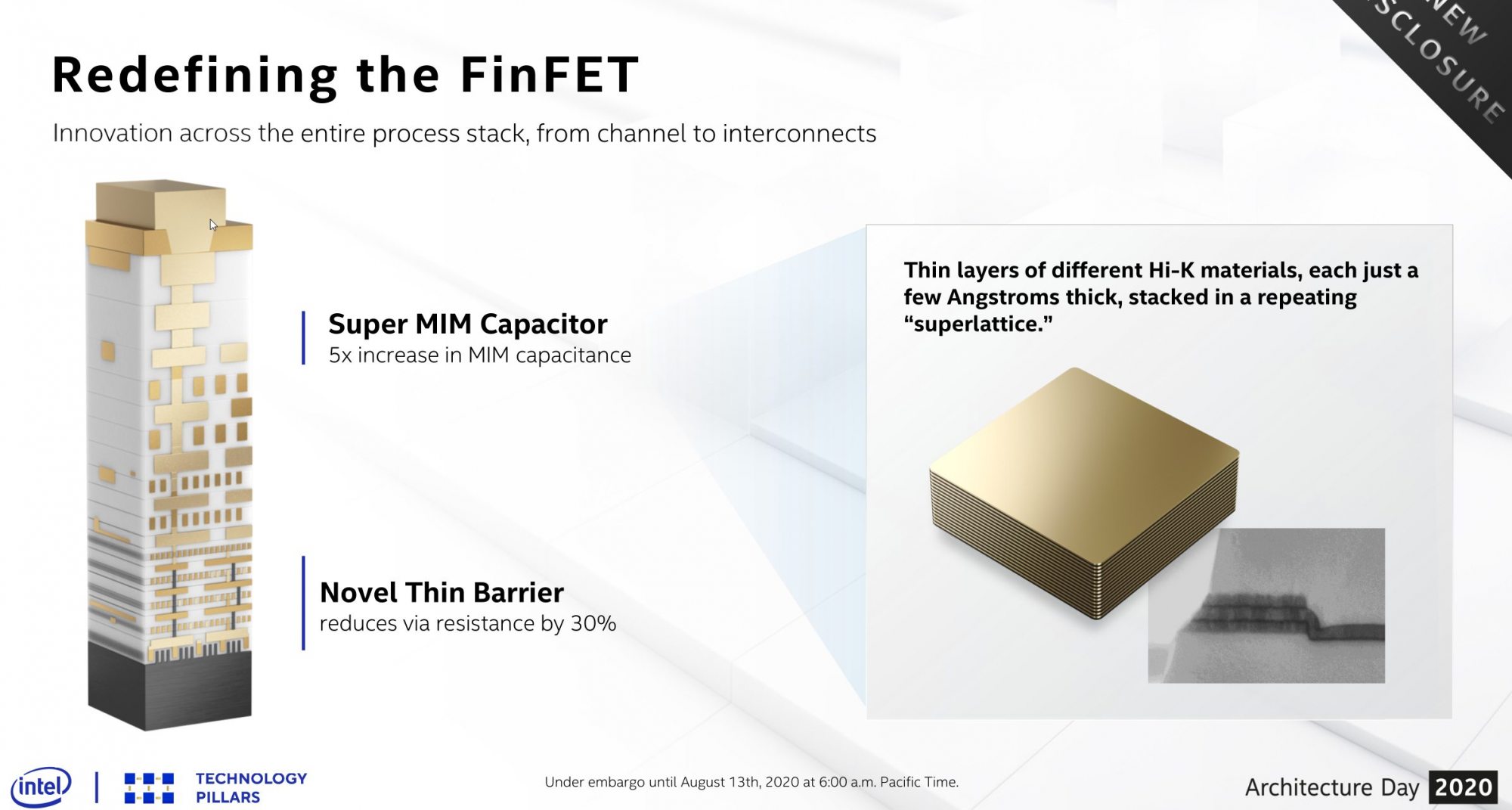
Its SuperFin transistors also see a new thin barrier that reduces the resistance by 30 per cent. Less resistance means more electric flow, which in turn increases performance and lowers power consumption.
To enhance power delivery, SuperFin uses a new metal-insulator-metal (MIM) capacitor that has five times higher capacitance. The new capacitor, called SuperMIM, features layers that are just a few Angstroms thick stacked in a “superlattice”. For an idea of its thickness, one Angstrom is equal to one ten-billionth of a metre, or the radius of a single silicon atom.
Intel said it is already preparing the next refinement of its 10nm process for 2021.


